Document #SPEC-3750A
Specifications are subject to change without notice.
GENERAL
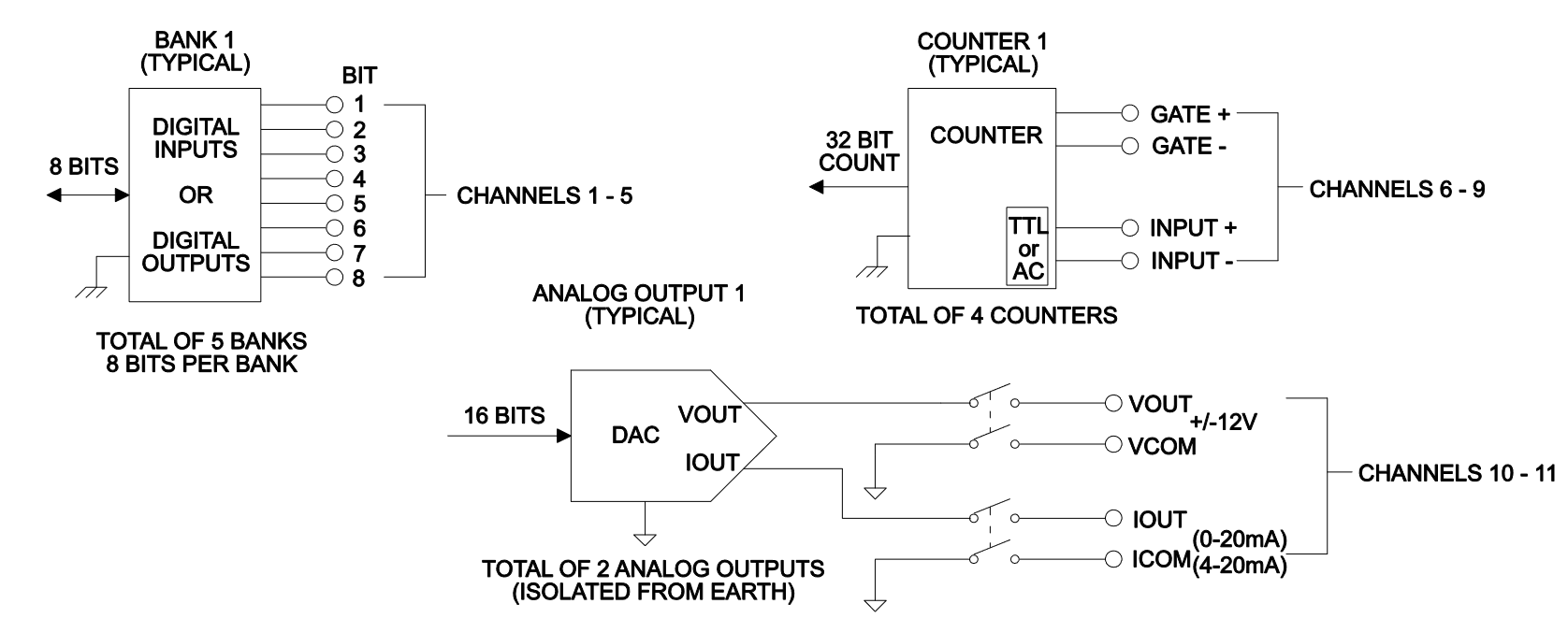
Channels 1 to 5: Bidirectional, high current digital I/O (40 bits)
Channels 6 to 9: 32-bit counter (4 counters)
Channels 10 to 11: Isolated voltage and current analog outputs (2 each)
DIGITAL I/O1
Configuration: 40 bidirectional digital I/O bits arranged in 5 banks of 8 bits each. Each bank can be configured for either input or output capability. 1 bank of I/O is equivalent to 1 system channel.
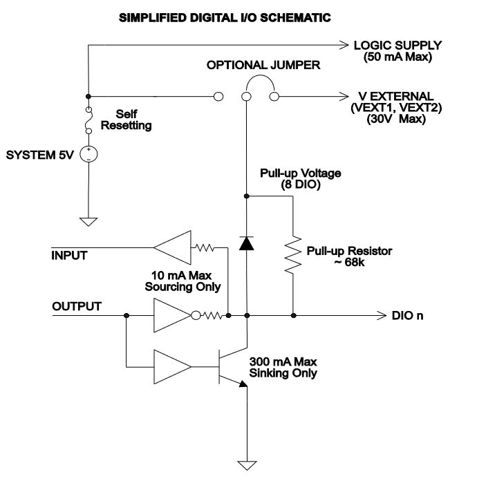
Digital Input specifications: An internal weak pull-up resistor of approximately 68 kΩ is provided on the card for each I/O. This pull-up resistor can be removed via onboard jumper on a channel (8 bit) basis. The pull-up voltage can either connect to the internally supplied 5V or an externally supplied voltage of up to 30V via onboard jumper. An internal 5V supply connection is separately available to run external logic circuits.
Digital Input logic low voltage: 0.8V max
Digital Input logic high voltage: 2V min.
Digital Input logic low current: −600μA max @ 0V
Digital Input logic high current: 50μA max @ 5V
Logic: Positive True.
System Input Minimum Read Speed2: 1000 readings / second.
Maximum externally supplied pull-up voltage: 30V
Maximum externally supplied voltage to any digital I/O line: Pull-up voltage (5V internal or up to 30V external)
Digital Output specifications: Each output has an internal fly-back diode for driving inductive loads. Each output is protected against continuous short circuits and over temperature. An internal 5V supply connection is separately available to run external logic circuits.
Digital Output logic high voltage: 2.4V minimum @ Iout = 10mA. sourcing only.
Digital Output logic low voltage: 0.5V maximum @ Iout = -300mA sinking only.
Maximum output sink current: 300mA per output, 3.0 A total per card.
Logic: Positive True.
System Output Minimum Write speed3: 1000 readings / second.
Maximum externally supplied voltage to any digital I/O line: Pull-up voltage (5V internal or up to 30V external)
Alarm: Trigger generation is supported for a maskable pattern match or state change on any of channels 1 through 5.
Protection: Optional disconnect (set to inputs) during output fault conditions.
Internal 5V logic supply: The internal logic supply is designed for powering external logic circuits of up to 50mA maximum. The logic supply is internally protected with a self-resetting fuse. Fuse reset time < 1 hour.
COUNTER / TOTALIZER INPUT
Maximum Count: 2 32 − 1
Maximum Input Rate: 1 MHz, rising or falling edge, programmable.
Minimum Input pulse width: 500 ns
Input Signal Level: 200 mVp-p (minimum), 42V Peak (maximum)
Threshold: AC (0V) or TTL Logic Level
Gate Input: TTL-HI (Gate+), TTL-LO (Gate-) or NONE.
Minimum Gate input setup time: 1us
Count Reset: Manual or Read + Reset
System Input Minimum Read speed: 1000 readings / second.
Alarm: Trigger generation is supported for a count match or counter overflow on any of channels 6 though 9
ANALOG VOLTAGE OUTPUT
The isolated analog voltage output is designed for general purpose, low power applications.
Output Amplitude4 ± 12V up to 10mA
Overload Current: 21mA minimum.
Resolution: 1mV.
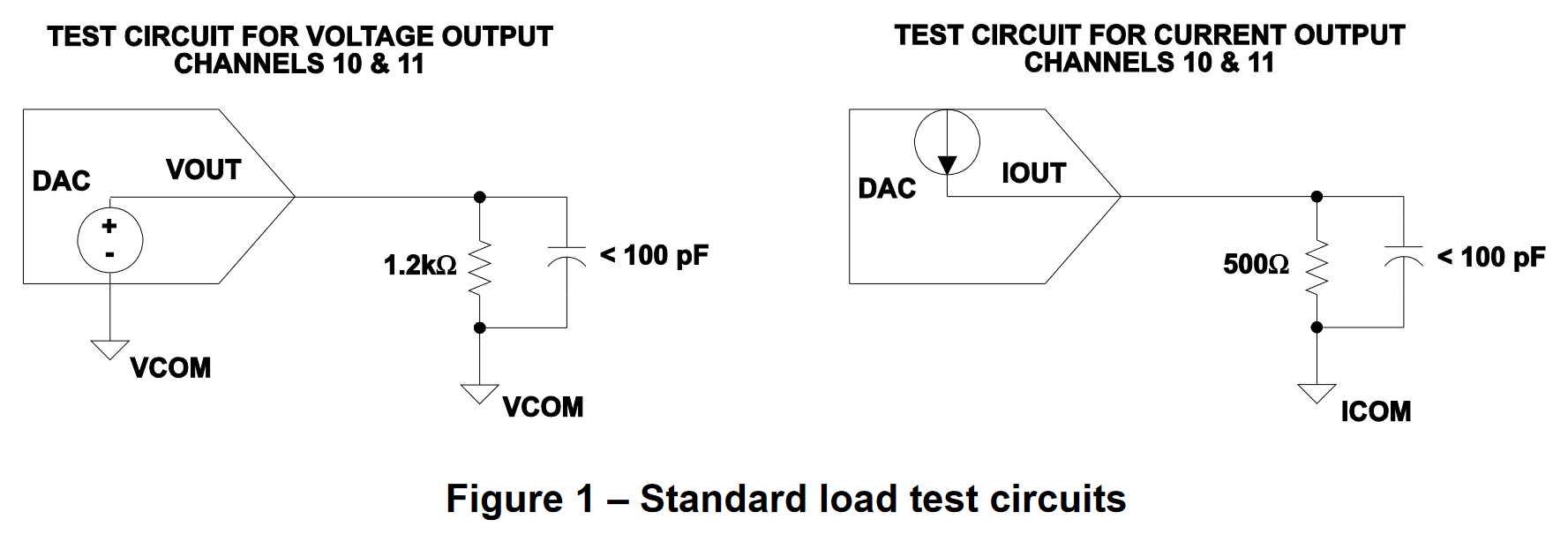
Full Scale Settling Time5: 1ms to 0.1% of output.
DC Accuracy6: ± (% of output + mV)
1 year 23 ± 5°C: 0.15% + 16mV
90 day 23 ± 5°C: 0.1% + 16mV
24 hour 23 ± 5°C: 0.04% + 16mV
Temperature Coefficient: ± (0.02% + 1.2mV) / °C
10mV Maximum Update Rate: 350us to 1% accuracy. System limited.
Output Fault Detection: System fault detection is available for short circuit output / current compliance.
Isolation: 300 V Peak Channel to Channel or Channel to Chassis.
Protection: Optional disconnect during output fault conditions.
Maximum guaranteed stable capacitive load: 10 nF
ANALOG CURRENT OUTPUT
The isolated analog current output is designed for 0-20 mA or 4-20 mA unipolar modes of operation.
Output Amplitude: 0 to 20mA or 4 to 20mA
Compliance Voltage: 11V minimum.
Maximum Open Circuit Voltage: 16V
Resolution: 1 µA.
Full Scale Settling Time5: 1ms to 0.1% of output.
DC Accuracy 7: ± (% of output + µA)
1 year 23 ± 5°C: 0.15% + 18µA
90 day 23 ± 5°C: 0.1% + 18µA
24 hour 23 ± 5°C: 0.04% + 18µA
Temperature Coefficient: ± (0.02% + 1.6uA) / °C
Output Fault Detection: System fault detection is available for open circuit output / voltage compliance.
Isolation: 300 V Peak Channel to Channel or Channel to Chassis.
Protection: Optional disconnect during output fault conditions.
CONNECTOR TYPE: Two 50 pin male D-shells.
OPERATING ENVIRONMENT:
Specified for 0°C to 50°C.
Specified to 70% R.H. at 35°C
STORAGE ENVIRONMENT: −25°C to 65°C
WEIGHT: 1.27 kg (2.80 lb)
FIRMWARE: Requires main revision to be 1.20 or above (applies to all 3706 series mainframes)
SAFETY: Conforms to European Union Directive 73/23/EEC, EN61010-1
EMC: Conforms to European Union Directive 2004/108/EC, EN61326-1
Power Budget Information:
Quiescent Power: 3300 mW
Digital Outputs each channel (1 through 5): 325 mW
Analog Channel each (10 & 11): 820 mW
Totalizer Channel all (6 through 9): 730 mW
Analog channels and counter channels may optionally be turned off to conserve system power.
See the Series 3700A Reference Manual for more detailed information.
1 All channels power up configured as inputs.
2 All channels configured as inputs.
3 All channels configured as outputs.
4 Programming up to 1% over full scale range is supported.
5 Measured with standard load shown in Figure 1.
6 Measured with > 10MΩ input DMM (DCV, filter, 1 PLC rate). Warm-up time is 1 hour @ 10mA load with 3750-ST.
7 Measured with < 2Ω shunt DMM (DCI, filter, 1 PLC rate). Warm-up time is 1 hour with 3750-ST.
Find more valuable resources at TEK.COM
Copyright © Tektronix. All rights reserved. Tektronix products are covered by U.S. and foreign patents, issued and pending. Information in this publication supersedes that in all previously published material. Specification and price change privileges reserved. TEKTRONIX and TEK are registered trademarks of Tektronix, Inc. All other trade names referenced are the service marks, trademarks or registered trademarks of their respective companies.
SPEC-3750 Rev. A / July 2008